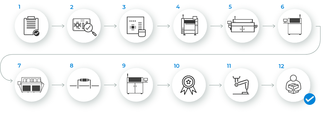
The following tasks must be completed before you receive your assembled PCBs.
1
Review order a) Confirm quantity and lead time b) Confirm solder paste type (lead or lead free) c) Confirm flux type (water soluble or no-clean) d) Review design files (Gerber files, BOM, centroid file, assembly drawings, etc.) e) Prepare assembly document.
2
Inspect PCBs and auditing parts.
3
Design and manufacturer SMT stencil(s) if PCB has SMT components.
4
Program pick and place machines to populate PCBs with SMT components. We use Mycronic MY300 for prototyping and Yamaha YSM20R for production.
5
Design thermal profile for PCBs.
6
Perform a visual and AOI inspection on each PCB. X-ray every leadless device (e.g. BGA and QFN).
7
Machine wash assembled PCBs with deionized water. Water soluble is our standard flux. Assembled PCBs with no-clean flux are not machine washed.
8
Insert through-hole component(s) if applicable.
9
Program selective soldering machine and solder through-hole components.
10
Perform a final QC inspection.
11
Perform functional test if applicable.
12
Package and ship assembled PCBs with any remaining material.