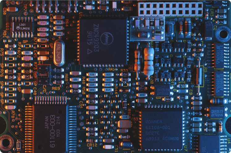
What is PCB Assembly?
PCB assembly, also known as printed circuit board assembly or PCBA, is the process of soldering electronic components onto a bare board to make a functional electronic circuit. Mixed technology refers to PCB assemblies require the use of surface mount and through-hole components.
The PCB assembly process for mixed technology assemblies can be divided into several stages:
Solder Paste Application
Solder paste is applied to the surface-mount pads on the bare PCB using a SMT stencil. The process of using a SMT stencil to apply solder paste to a bare PCB is called printing. It can be done with an automatic or manual stencil printer.
*We only use automatic stencil printers.
SMT Component Placement
SMT components are usually placed onto the bare boards using an automatic pick and place machine. The machine first needs to be programmed using the project’s BOM (bill of material) and XY data. The BOM contains a list of all the manufacturer or vendor part numbers, reference designators and other part related information associated with a particular PCB. The XY data contains the coordinates and rotation of each part on the BOM.
*We use Mycronic pick and place machines for prototype PCB assembly and Yahama pick and place machines for production assembly.
Reflow Soldering
In surface-mount technology (SMT), the most common method is reflow soldering. A typical reflow oven contains multiple zones with heating elements. The PCB is heated in a controlled manner causing the solder paste to melt and form a liquid state. The liquid solder then solidifies as it cools, creating the solder joints that connect the components to the PCB.
Through-hole Soldering
Some components have leads that pass through plated holes drilled in the PCB. Through-hole components require a different soldering technique. The leads are inserted through the holes, and the solder is applied on the opposite side of the PCB using a number of tools including a soldering iron, a soldering robot, a selective soldering machine or a wave solder machine.
Visual and Testing
We inspect your printed circuit boards at various stages of the manufacturing/assembly process for early detection of faults. Correcting defects at an early stage improves yields during the PCB testing stage. We use visual inspection, automated optical inspection (AOI) and automated X-ray inspection. After the boards have been manufactured and have passed all the PCB assembly inspections, they are ready for testing.
Cleaning and Finishing
Depending on the requirements, the PCB assembly may go through a cleaning process to remove any flux residues or contaminants. It may also undergo additional processes like conformal coating or encapsulation for protection against environmental factors.
The PCB assembly process requires expertise, precision, and adherence to industry standards. The complexity and scale of the assembly process can vary, ranging from simple prototypes to high-volume production runs for consumer electronics, industrial equipment, automotive applications, and more.
LEAVE A REPLY