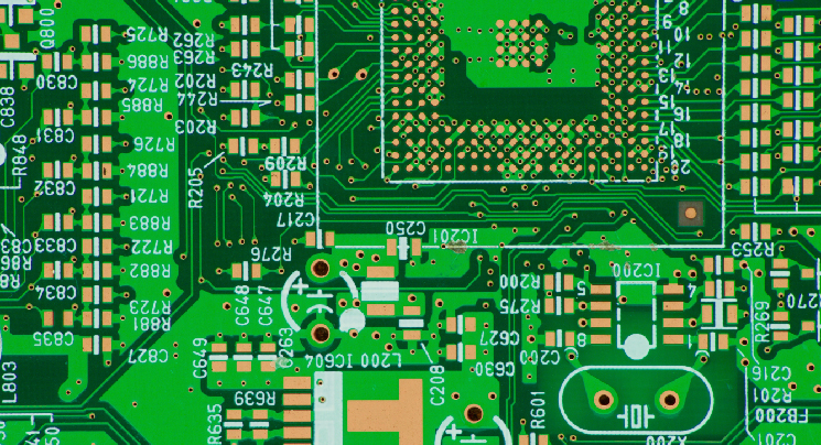
Introduction to Printed Circuit Board Assembly (PCBA)
PCB
Assembly, also known as PCB Soldering, refers to the process of soldering
electronic components to a printed circuit board (PCB).The process used to
solder SMT (Surface Mount Technology) components is different than the one used
to solder through-hole components.
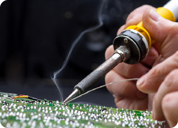
What is Soldering?
Soldering is a process in which electronic components are joined to a printed circuit board using a metal alloy known as solder. Solder has a relative low melting point (e.g. lower than the adjoining metals). When solder is heated up beyond its melting temperature it melts. When it cools down it create an electrical bond known as solder joint.
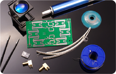
Soldering tools
The basic tools require for soldering are:
1. Wire Solder and/or Solder Paste
2. Solder Flux
3. A soldering Iron if you are using wire solder. A SMT stencil and a heat source like a hotplate or a reflow oven if you are using solder paste.
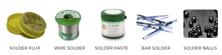
Solder Flux is a chemical cleaning agent used during the soldering process. It removes the oxides present on the metal surface and prevents re-oxidation during the soldering process. By preventing the formation of metal oxides, flux enables the solder to adhere to the clean metal surface.
There are many kinds of solder but there are only three categories, lead base solder, lead free solder and flux core solder. The most common type of packaging are wire solder, solder paste, solder bar and solder balls.
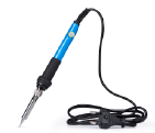
A soldering iron is a hand tool that supplies heat to melt the solder so it can flow between the pieces needed to be soldered. It consists of a metal tip and an insulated handle. The tip is applied to the wire solder while holding the iron by the insulated handle.
SMT versus Through-hole Soldering
Through-hole Soldering – the component leads are inserted into the drilled plated holes on a printed circuit board and soldered to pads on the opposite side either by manual assembly (using a soldering iron) or by the use of an automated machine (e.g. a wave or selective soldering machine). Through-hole components are used for high-reliability products that require stronger connections between layers.
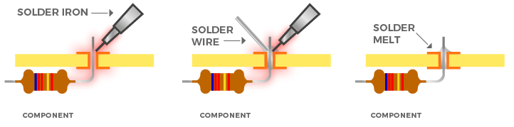
SMT Soldering – the components are mounted directly onto the surface of a printed circuit board. Some SMT components can be soldered manually with a soldering iron, but most of them are too small to solder manually and require hot-air solder reflow equipment.
PCB Assembly using automated equipment
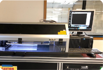
In this day and age, most original equipment manufacturers (OEM) and electronic contract manufacturers have to use automated equipment to solder electronic components to printed circuit boards. Furthermore, the equipment used to deal with SMT components is completely different than that used for through-hole components. Depending on the production volume, companies have one or more SMT lines. A typical SMT line has the following configuration: an automated stencil printer, an automated pick and place machine and a reflow oven with multiple zones. Our SMT lines include an automated optical inspection machine (AOI).
The SMT process
Printing is the first step of the SMT process, an automated stencil printer is used to apply the solder paste on the bare PCBs. Mechanical fixtures inside the printer hold the PCB and the SMT stencil together, the pads on the PCB and the apertures on the stencils are perfectly aligned using the printer’s vision system. The thickness of the stencil, the size of the apertures, the pressure and velocity of the squeegee blade control the amount of paste deposited on the SMT pads on the PCBs.
Placement is the second step of the SMT, an automatic “Pick and Place” machine is used to place the SMT the components on the PCBs. On this machine, a robotic device places components on the PCB automatically. Before this can happen, the machine needs to be programmed using the design files (Gerber files, BOM and CAD file also known as XY Data). The CAD file contains the location and rotation information of all the components on the BOM.
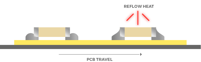
Reflow soldering is the third step of the SMT process, the PCBs are sent through a reflow oven. The solder paste works as a bonding agent holding the components during heating. The oven is programmed with a thermal profile that corresponds to the solder paste in used. Once the paste reaches its reflow temperature it melts. In the case of double-side boards, each side has to be done individually.
Typical SMT line configuration
Loader: automatically loads the PCBs to the stencil printer.
Stencil Printer: applies solder paste to the bare boards.
Inspection Conveyor: used to inspect the solder paste on the boards as they come out of the stencil printer.
Pick and Place Machine: places the SMT components on the boards.
Inspection Conveyor: used to inspect placements of components on the boards.
Reflow Oven: used to solder the components on the boards.
Unloader: automatically unloads the
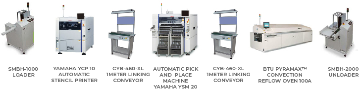
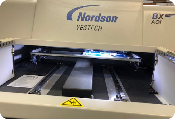
After
SMT the boards are visually inspected. PCB Assembly Express also performs a
second inspection using an automatic optical inspection (AOI) machine.
When the boards have leadless devices (e.g. BGA and QFN) they need to be inspected using an x-ray machine to conform to IPC standards.
Through-hole process
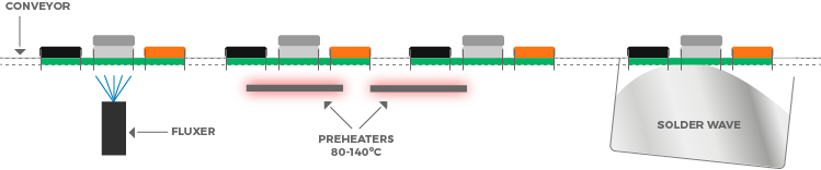
When the PCBs have through-hole components, there are two different type of equipment commonly used for soldering, wave soldering machines and selective soldering machines.
Wave soldering is the preferred method when soldering a large number of through-hole components. During wave soldering, the PCBs are passed over a wave of molten solder. The components become soldered to the boards as the PCBs make contact with the wave,. When working with double-sided boards special fixtures known as wave pallets can used to prevent solder from going to areas of the boards with SMT components.
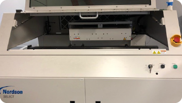
Selective soldering is the preferred method when soldering mixed technology PCBs and the boards do not have a lot of through-hole components. During this process, individual through-hole components are soldered on a PCB using a solder fountain. The components to be selectively soldered are usually surrounded by components that have been previously soldered during the surface-mount reflow process.
After
the through-hole process the PCBs are visually inspected again. They can also
be inspected with an AOI machine.
Final quality inspection
After the boards are washed (if water soluble flux was used) and depanelized (if the boards were panelized) they go through a final visual inspection before they are packaged and shipped. The boards are inspected according to their class designation: Class 1 – General Electronic Products, Class 2 – Dedicated Service Electronic Products, and Class 3 – High Reliability Electronic Products.
PCB testing
In-circuit testing (ICT) and functional testing (FCT) are two of the most popular testing methods. ICT, also known as bed-of-nails, can be used to test individual components and measure their performance. It can almost provide 100% coverage. FCT helps ensure that the PCBs function properly according to the project’s specifications and that they do not have defects.
LEAVE A REPLY