
Keys for a Successful PCB Assembly Project
When hiring a PCB assembly contract manufacturer, many clients overlook the importance of providing the printed circuit board and component data in a proper way and format. Any missing information will cause delays in your order. In this article we discuss some of the most critical concepts to ensure a successful and painless experience when ordering PCB assembly services.

Panelization
Panelization is the process of arranging multiple circuit boards on a single panel. This is done to increase the efficiency of the assembly and to reduce the cost of circuit boards. By panelizing the boards, multiple boards can be processed at the same time, which speeds up the assembly labor.
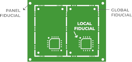
PCB Fiducials
Fiducials are small marks on a circuit board that are used as reference points during the PCB assembly process. They are usually located in the corners of the board and are used to align the board with the pick and place machine, which is used to place the components onto the board. Fiducials are essential for ensuring that the components are placed in the correct location, which is crucial for the proper functioning of the circuit board.
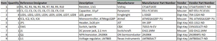
Bill of Materials (BOM)
A Bill of Materials, or BOM, is a comprehensive list of all the components that are required to assemble a printed circuit board. At a minimum, it should include the quantity, reference designators, and manufacturer part numbers for each component. Providing a detailed and accurate BOM is essential to ensure that all the necessary components are available for assembly and to keep track of inventory.
A good bill of materials should have, at least, the following information:
- Manufacturer part number: Each component should have a unique part number that can be easily referenced and tracked.
- Manufacturer: The name of the manufacturer of each component.
- Quantity: The number of each component needed for the PCB assembly.
- Description: A clear and detailed description of each component, including its function and specifications.
- Reference designators: A string of characters, usually letters followed by a number, such as R1, C1, C2, U7, etc., that are used to identify each component on the PCB layout.
It is desirable (but not required) to include the following:
- Vendor: The name of the vendor or supplier from where the component can be purchased.
- Footprint: The name of the footprint or physical dimensions of each component, including the size and shape of the pads on the printed circuit board.
- Packaging: The mounting type of each component, such as a through-hole or surface-mount.
- Datasheet: A link or reference to the datasheet or technical specification of each component.
- Cost: The cost of each component, which can be used for budgeting and cost estimation.
- Alternate components: Alternate components that can be used as substitutes for the primary components when the original is unavailable.
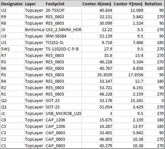
Pick and Place Data
Pick and Place (PnP) files are used by the pick and place machine to determine the location of each component on the circuit board. These files are created by the designer and contain the coordinates of each component on the board, as well as the reference designator and rotation. PnP files are essential for ensuring that the components are placed in the correct location on the board.
A good PCB pick and place file should have the following information:
• A list of all components, including their reference designators and values.
• The x, y coordinates for the location of each component on the printed circuit board.
• The rotation angle for each component.
• The layer on which each component is placed (Top or Bottom).
• The footprint or package type for each component.
• Any additional information required by the pick and place machine, such as feeder information or component height.
Need Help?
PCB Assembly Express offers quick-turn prototype PCB assembly services as well as production PCB assembly services. Our customer service team is available by phone or by email 8:00 am to 5:00 pm Monday through Friday. Please contact us if you have any questions on how to prepare your data for a successful and smooth PCB assembly project.
LEAVE A REPLY