
SMT Stencil Design in the PCB Assembly Process
Stencil design is a critical step in the PCB assembly process, but it doesn’t always get the attention it should. The stencil controls the precise amount of solder paste deposited onto each pad which directly impacts solder joint quality, assembly yield, and overall product reliability.
A well-designed stencil can reduce defects such:
- Component Misalignment
- Insufficient Solder Joints
- Solder bridging
- Tombstoning
- Voiding Under Components
- Solder Skipping
PCB Assembly Express works closely with Stencils Unlimited to provide optimized SMT stencil designs. Each stencil is carefully tailored to your PCB layout, component mix, and assembly requirements. They:
- Review stencil design as part of DFM analysis
- Optimize thickness based on component mix
- Apply aperture modifications where needed
- Ensure compatibility with assembly process
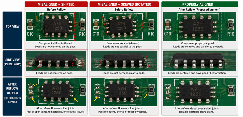
Component Misalignment (Shifting and Skewing)
This occurs when an SMT component is not properly positioned on the printed circuit board after placement or reflow in the PCB assembly process. It may shift (move off its pads) or skew (rotate out of alignment), resulting in poor solder joints and potential electrical issues. A properly designed stencil helps reduce this misalignment by providing uniform solder paste deposition, creating balanced surface tension forces during reflow to keep components centered on their pads.
Insufficient Solder Joints?
This occurs when there isn’t enough solder on a pad to properly connect the component lead, resulting in weak or incomplete connections that can cause electrical failures. In the PCB assembly process, a properly designed stencil helps prevent insufficient solder joints by ensuring the correct amount of solder paste is deposited on each pad for strong and reliable connections.
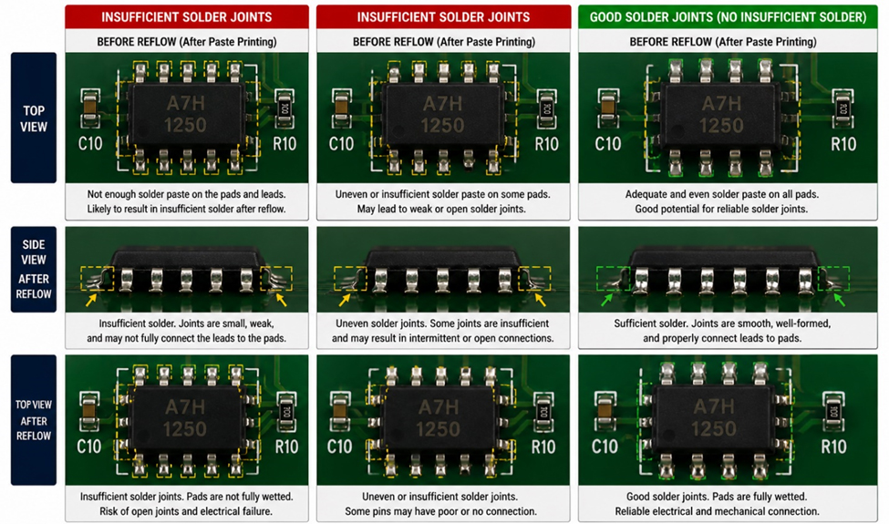
Figure 2. Insufficient Solder Joints
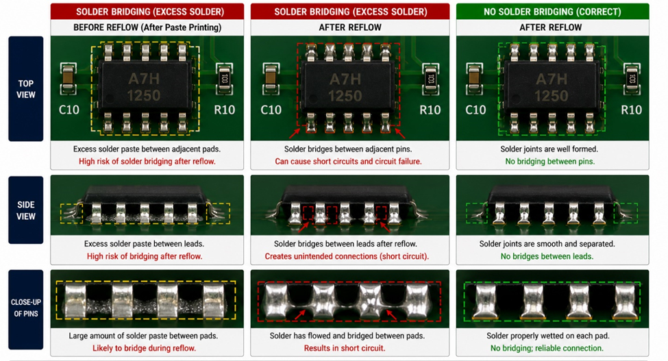
Solder Bridging?
This occurs when excess solder unintentionally connects two nearby pads or component leads, creating a short circuit that can cause the circuit to malfunction. In the PCB assembly process, a properly designed stencil helps prevent solder bridging by depositing the right amount of solder paste in the correct locations, reducing the chance of solder flowing between adjacent pads during reflow.
Tombstoning
This occurs when a small surface-mount component (such as a resistor or capacitor) lifts up on one end during soldering in the PCB assembly process, standing upright instead of lying flat on the printed circuit board, which can lead to a poor or open electrical connection. A properly designed stencil helps reduce tombstoning by ensuring equal solder paste is deposited on both pads, creating balanced forces during reflow and keeping the component flat.
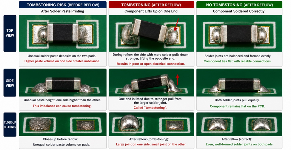
Figure 4. Tombstonig
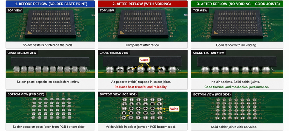
Voiding Under Components
This occurs when
small air pockets or gaps form inside the solder joint beneath a component,
which can weaken the connection and reduce heat transfer.
A properly designed stencil reduces voiding by controlling solder paste volume
and using segmented aperture patterns that allow trapped gases to escape during
reflow.
Solder Skipping
This occurs when solder does not properly adhere to part of a pad or component lead during the PCB assembly process, leaving areas without solder. A properly designed stencil helps reduce solder skipping by ensuring consistent and sufficient solder paste deposition on every pad, allowing the solder to entirely wet the leads and form complete, reliable joints during reflow.
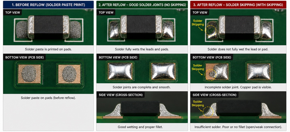
Figure 6. Solder Skipping
SMT Stencil Types
Choosing the right stencil type helps achieve consistent results across different component sizes and layout densities.
Standard
Laser-Cut Stainless-Steel Stencil:
This stencil has a uniform thickness and is used for most SMT assemblies
without large pitch variation. It also offers the lowest lead time and
manufacturing cost.
Step Stencil
(Step-Up / Step-Down):
This stencil has varying thicknesses in specific areas to increase or decrease
solder paste volume for mixed component sizes.
Electroformed
Stencil:
This stencil offers very smooth aperture walls for improved paste release,
making it ideal for fine-pitch and high-density designs; however, its thickness
is not as uniform as that of a standard stencil.
Nano-Coated
Stencil:
This stencil has a special surface treatment that enhances paste release by
reducing solder paste adhesion to the stencil walls. It also reduces the
frequency of stencil cleaning.
Stencil Thickness
Stencil thickness determines how much solder paste is deposited. Choosing the right thickness is essential for balancing solder volume across all components.
- Small pads require thinner stencils to avoid excess solder
- Large pads may require thicker stencils for proper solder joints
Typical Thickness Guidelines
- 0.004″ (100 µm) ? Fine-pitch components (e.g., QFNs, BGAs)
- 0.005″ (125 µm) ? Most common, general-purpose designs
- 0.006″ (150 µm) ? Larger components or higher solder volume needs
Aperture Design & Modifications
Stencil apertures (openings) control how much solder paste goes onto each pad. Proper aperture design helps prevent defects.
Aperture
Reduction:
Aperture reduction makes the stencil opening smaller than the pad to control
how much solder paste is applied and prevent defects like solder bridging.
Reducing the aperture size by about 5–20% helps limit excess solder and is
commonly used for fine-pitch components, QFNs, and BGAs.
Home Plate
Apertures:
Home plate apertures use a trapezoidal shape to reduce the amount of solder
paste at the front edge of chip components, helping prevent tombstoning by
controlling how the solder pulls during reflow.
Window Pane
Apertures:
Window pane apertures divide large stencil openings into smaller sections to
better control solder paste on large pads, such as thermal pads. This design
helps reduce voiding, improves paste release, and prevents components from
floating during reflow.
Rounded
Apertures:
Rounded apertures improve solder paste release from the stencil by reducing
sharp corners where paste tends to stick.
Overprint
Apertures:
Overprint apertures are slightly larger than the pad to increase solder volume
where additional solder is needed for stronger joints.
Step
Aperture Modifications:
Step aperture modifications locally adjust paste volume by varying stencil
thickness or aperture design to accommodate mixed component sizes.
LEAVE A REPLY